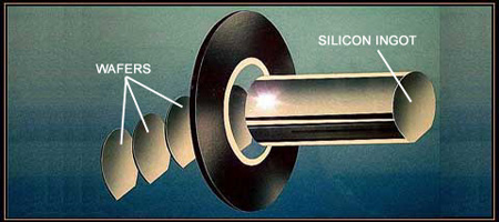
To slice crystal ingot into uniformly thin slices (wafers) of specific thickness and warpage in high precision.
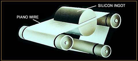
Wire Saw
A fine high tensile wire is used as a medium carrying abrasive slurry abrading through the ingot. The whole ingot is being sliced simultaneously into hundreds of wafers by one single wire wound continuously in multiple loops.
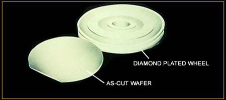
2. Grinding
Edge-Grinding
Mechanical grinding to round up the wafer's edge to minimize physical damage in downstream processes and to prevent edge crowning in the case of Epitaxial growth.
Custom built precision grinding machine utilizing fine grit diamond grinding wheel, produces a uniform and smooth edge profile.
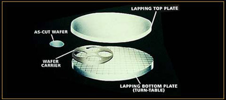
To remove the physical irregularities and crystal damage layer left by slicing to create perfectly flat surface and uniform thickness.
Wafers are sandwiched between two perfectly flat rotating plates in the presence of abrasive slurry - abrasion and removal on both sides simultaneously.
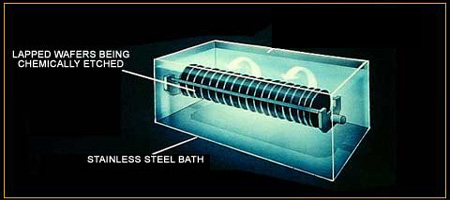
4. Etching
To chemically etch off a layer from the surface, the underlying damage layer left by lapping to produce a damage-free perfect crystal structure on the surface.
Lapped wafers are immersed and rotated in a chemical bath with precisely controlled parameters - viz. chemical strength, temperature, flow-pattern, etc.
A fully automated custom built machine, integrating several processes - cleaning, etching, rinsing, drying, etc. into one.
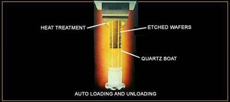
To eliminate the thermal donors (electrons) left over from crystal growth and various processing, to restore the natural electrical properties of the crystal.
Extremely clean wafers undergo heat treatment in super clean dust-free furnace made of super pure quartz.
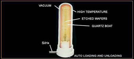
To deposit a thin film of polysilicon (about 1 micron) on the back surface of the wafer - to create an extrinsic gettering effect of attracting impurities away from the IC fabricating surface to the back surface.
Polysilicon film deposited from Silane (SiH4) in super clean dust-free CVD furnace made of super pure quartz in cleanest possible environment.
Note : PBS = Poly-Back Seal , CVD = Chemical Vapor Deposition
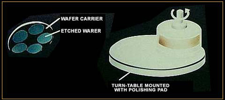
To polish the edge surface to mirror finish to minimize adhesion and generation of particles (when wafers rub against carrier cassettes during IC fabrication process.
Wafer edge is polished by a chemical-mechanical process using high precision silica matrix wheel and chemical slurry.
To produce a super flat mirror surface microscopically smooth and free from any crystal damage or imperfection, to cater for the most stringent IC fabrication requirements.
A chemical-mechanical process using fabric pad in fine colloidal alkaline medium.
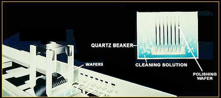
9. Cleaning
Remove all forms of physical and ionic contaminations such as microscopic particles and metallic / non-metallic matters to create cleanest possible surface for the most sophisticated IC fabrication requirements.
A multi-step cassetteless cleaning system using super-pure deionised water, high-purity grade chemicals and ultra-sonic vibrators in a class one clean ambience.
10. Inspection
The super-clean wafers are then inspected for surface defect with the aid of collomated light in a darkened dust-free environment and with the aid of advance inspection equipment, the wafer's properties are carefully inspected to ensure strict adherence to the customer's requirements.
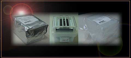
11. Packing
The accepted wafers are packed in a specially designed package with stringent emphasis on the cleanliness of the wafers. Packing the wafers are done in a dust and moist-free environment. The package must also hold the wafers securely so that they will not rattle inside which may induce particles from the container or wafers themselves.